Combining next-token prediction and video diffusion in computer vision and robotics

In the current AI zeitgeist, sequence models have skyrocketed in popularity for their ability to analyze data and predict what to do next. For instance, you’ve likely used next-token prediction models like ChatGPT, which anticipate each word (token) in a sequence to form answers to users’ queries. There are also full-sequence diffusion models like Sora, which convert words into dazzling, realistic visuals by successively “denoising” an entire video sequence. 

Researchers from MIT’s Computer Science and Artificial Intelligence Laboratory (CSAIL) have proposed a simple change to the diffusion training scheme that makes this sequence denoising considerably more flexible.

When applied to fields like computer vision and robotics, the next-token and full-sequence diffusion models have capability trade-offs. Next-token models can spit out sequences that vary in length. However, they make these generations while being unaware of desirable states in the far future — such as steering its sequence generation toward a certain goal 10 tokens away — and thus require additional mechanisms for long-horizon (long-term) planning. Diffusion models can perform such future-conditioned sampling, but lack the ability of next-token models to generate variable-length sequences.

Researchers from CSAIL want to combine the strengths of both models, so they created a sequence model training technique called “Diffusion Forcing.” The name comes from “Teacher Forcing,” the conventional training scheme that breaks down full sequence generation into the smaller, easier steps of next-token generation (much like a good teacher simplifying a complex concept).

Diffusion Forcing found common ground between diffusion models and teacher forcing: They both use training schemes that involve predicting masked (noisy) tokens from unmasked ones. In the case of diffusion models, they gradually add noise to data, which can be viewed as fractional masking. The MIT researchers’ Diffusion Forcing method trains neural networks to cleanse a collection of tokens, removing different amounts of noise within each one while simultaneously predicting the next few tokens. The result: a flexible, reliable sequence model that resulted in higher-quality artificial videos and more precise decision-making for robots and AI agents.

By sorting through noisy data and reliably predicting the next steps in a task, Diffusion Forcing can aid a robot in ignoring visual distractions to complete manipulation tasks. It can also generate stable and consistent video sequences and even guide an AI agent through digital mazes. This method could potentially enable household and factory robots to generalize to new tasks and improve AI-generated entertainment.

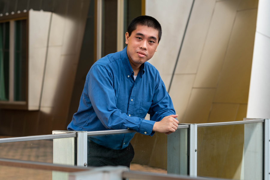
“Sequence models aim to condition on the known past and predict the unknown future, a type of binary masking. However, masking doesn’t need to be binary,” says lead author, MIT electrical engineering and computer science (EECS) PhD student, and CSAIL member Boyuan Chen. “With Diffusion Forcing, we add different levels of noise to each token, effectively serving as a type of fractional masking. At test time, our system can “unmask” a collection of tokens and diffuse a sequence in the near future at a lower noise level. It knows what to trust within its data to overcome out-of-distribution inputs.”

In several experiments, Diffusion Forcing thrived at ignoring misleading data to execute tasks while anticipating future actions.

When implemented into a robotic arm, for example, it helped swap two toy fruits across three circular mats, a minimal example of a family of long-horizon tasks that require memories. The researchers trained the robot by controlling it from a distance (or teleoperating it) in virtual reality. The robot is trained to mimic the user’s movements from its camera. Despite starting from random positions and seeing distractions like a shopping bag blocking the markers, it placed the objects into its target spots.

To generate videos, they trained Diffusion Forcing on “Minecraft” game play and colorful digital environments created within Google’s DeepMind Lab Simulator. When given a single frame of footage, the method produced more stable, higher-resolution videos than comparable baselines like a Sora-like full-sequence diffusion model and ChatGPT-like next-token models. These approaches created videos that appeared inconsistent, with the latter sometimes failing to generate working video past just 72 frames.

Diffusion Forcing not only generates fancy videos, but can also serve as a motion planner that steers toward desired outcomes or rewards. Thanks to its flexibility, Diffusion Forcing can uniquely generate plans with varying horizon, perform tree search, and incorporate the intuition that the distant future is more uncertain than the near future. In the task of solving a 2D maze, Diffusion Forcing outperformed six baselines by generating faster plans leading to the goal location, indicating that it could be an effective planner for robots in the future.

Across each demo, Diffusion Forcing acted as a full sequence model, a next-token prediction model, or both. According to Chen, this versatile approach could potentially serve as a powerful backbone for a “world model,” an AI system that can simulate the dynamics of the world by training on billions of internet videos. This would allow robots to perform novel tasks by imagining what they need to do based on their surroundings. For example, if you asked a robot to open a door without being trained on how to do it, the model could produce a video that’ll show the machine how to do it.

The team is currently looking to scale up their method to larger datasets and the latest transformer models to improve performance. They intend to broaden their work to build a ChatGPT-like robot brain that helps robots perform tasks in new environments without human demonstration.

“With Diffusion Forcing, we are taking a step to bringing video generation and robotics closer together,” says senior author Vincent Sitzmann, MIT assistant professor and member of CSAIL, where he leads the Scene Representation group. “In the end, we hope that we can use all the knowledge stored in videos on the internet to enable robots to help in everyday life. Many more exciting research challenges remain, like how robots can learn to imitate humans by watching them even when their own bodies are so different from our own!”

Chen and Sitzmann wrote the paper alongside recent MIT visiting researcher Diego Martí Monsó, and CSAIL affiliates: Yilun Du, a EECS graduate student; Max Simchowitz, former postdoc and incoming Carnegie Mellon University assistant professor; and Russ Tedrake, the Toyota Professor of EECS, Aeronautics and Astronautics, and Mechanical Engineering at MIT, vice president of robotics research at the Toyota Research Institute, and CSAIL member. Their work was supported, in part, by the U.S. National Science Foundation, the Singapore Defence Science and Technology Agency, Intelligence Advanced Research Projects Activity via the U.S. Department of the Interior, and the Amazon Science Hub. They will present their research at NeurIPS in December.

MIT team takes a major step toward fully 3D-printed active electronics

Active electronics — components that can control electrical signals — usually contain semiconductor devices that receive, store, and process information. These components, which must be made in a clean room, require advanced fabrication technology that is not widely available outside a few specialized manufacturing centers.

During the Covid-19 pandemic, the lack of widespread semiconductor fabrication facilities was one cause of a worldwide electronics shortage, which drove up costs for consumers and had implications in everything from economic growth to national defense. The ability to 3D print an entire, active electronic device without the need for semiconductors could bring electronics fabrication to businesses, labs, and homes across the globe.

While this idea is still far off, MIT researchers have taken an important step in that direction by demonstrating fully 3D-printed resettable fuses, which are key components of active electronics that usually require semiconductors.

The researchers’ semiconductor-free devices, which they produced using standard 3D printing hardware and an inexpensive, biodegradable material, can perform the same switching functions as the semiconductor-based transistors used for processing operations in active electronics.

Although still far from achieving the performance of semiconductor transistors, the 3D-printed devices could be used for basic control operations like regulating the speed of an electric motor.

“This technology has real legs. While we cannot compete with silicon as a semiconductor, our idea is not to necessarily replace what is existing, but to push 3D printing technology into uncharted territory. In a nutshell, this is really about democratizing technology. This could allow anyone to create smart hardware far from traditional manufacturing centers,” says Luis Fernando Velásquez-García, a principal research scientist in MIT’s Microsystems Technology Laboratories (MTL) and senior author of a paper describing the devices, which appears in Virtual and Physical Prototyping.

He is joined on the paper by lead author Jorge Cañada, an electrical engineering and computer science graduate student.

An unexpected project

Semiconductors, including silicon, are materials with electrical properties that can be tailored by adding certain impurities. A silicon device can have conductive and insulating regions, depending on how it is engineered. These properties make silicon ideal for producing transistors, which are a basic building block of modern electronics.

However, the researchers didn’t set out to 3D-print semiconductor-free devices that could behave like silicon-based transistors.

This project grew out of another in which they were fabricating magnetic coils using extrusion printing, a process where the printer melts filament and squirts material through a nozzle, fabricating an object layer-by-layer.

They saw an interesting phenomenon in the material they were using, a polymer filament doped with copper nanoparticles.

If they passed a large amount of electric current into the material, it would exhibit a huge spike in resistance but would return to its original level shortly after the current flow stopped.

This property enables engineers to make transistors that can operate as switches, something that is typically only associated with silicon and other semiconductors. Transistors, which switch on and off to process binary data, are used to form logic gates which perform computation.

“We saw that this was something that could help take 3D printing hardware to the next level. It offers a clear way to provide some degree of ‘smart’ to an electronic device,” Velásquez-García says.

The researchers tried to replicate the same phenomenon with other 3D printing filaments, testing polymers doped with carbon, carbon nanotubes, and graphene. In the end, they could not find another printable material that could function as a resettable fuse.

They hypothesize that the copper particles in the material spread out when it is heated by the electric current, which causes a spike in resistance that comes back down when the material cools and the copper particles move closer together. They also think the polymer base of the material changes from crystalline to amorphous when heated, then returns to crystalline when cooled down — a phenomenon known as the polymeric positive temperature coefficient.

“For now, that is our best explanation, but that is not the full answer because that doesn’t explain why it only happened in this combination of materials. We need to do more research, but there is no doubt that this phenomenon is real,” he says.

3D-printing active electronics

The team leveraged the phenomenon to print switches in a single step that could be used to form semiconductor-free logic gates.

The devices are made from thin, 3D-printed traces of the copper-doped polymer. They contain intersecting conductive regions that enable the researchers to regulate the resistance by controlling the voltage fed into the switch.

While the devices did not perform as well as silicon-based transistors, they could be used for simpler control and processing functions, such as turning a motor on and off. Their experiments showed that, even after 4,000 cycles of switching, the devices showed no signs of deterioration.

But there are limits to how small the researchers can make the switches, based on the physics of extrusion printing and the properties of the material. They could print devices that were a few hundred microns, but transistors in state-of-the-art electronics are only few nanometers in diameter.

“The reality is that there are many engineering situations that don’t require the best chips. At the end of the day, all you care about is whether your device can do the task. This technology is able to satisfy a constraint like that,” he says.

However, unlike semiconductor fabrication, their technique uses a biodegradable material and the process uses less energy and produces less waste. The polymer filament could also be doped with other materials, like magnetic microparticles that could enable additional functionalities.

In the future, the researchers want to use this technology to print fully functional electronics. They are striving to fabricate a working magnetic motor using only extrusion 3D printing. They also want to finetune the process so they could build more complex circuits and see how far they can push the performance of these devices.

“This paper demonstrates that active electronic devices can be made using extruded polymeric conductive materials. This technology enables electronics to be built into 3D printed structures. An intriguing application is on-demand 3D printing of mechatronics on board spacecraft,” says Roger Howe, the William E. Ayer Professor of Engineering, Emeritus, at Stanford University, who was not involved with this work.

This work is funded, in part, by Empiriko Corporation.

New 3D printing technique creates unique objects quickly and with less waste

Multimaterial 3D printing enables makers to fabricate customized devices with multiple colors and varied textures. But the process can be time-consuming and wasteful because existing 3D printers must switch between multiple nozzles, often discarding one material before they can start depositing another.

By modulating the speed of the second nozzle, which applies heat to a temperature-responsive filament, the researchers can vary the shade of materials to create objects with complex patterns, without the need to use multiple materials. Photo courtesy of the researchers.

Researchers from MIT and Delft University of Technology have now introduced a more efficient, less wasteful, and higher-precision technique that leverages heat-responsive materials to print objects that have multiple colors, shades, and textures in one step.

Their method, called speed-modulated ironing, utilizes a dual-nozzle 3D printer. The first nozzle deposits a heat-responsive filament and the second nozzle passes over the printed material to activate certain responses, such as changes in opacity or coarseness, using heat.

By controlling the speed of the second nozzle, the researchers can heat the material to specific temperatures, finely tuning the color, shade, and roughness of the heat-responsive filaments. Importantly, this method does not require any hardware modifications.

The researchers developed a model that predicts the amount of heat the “ironing” nozzle will transfer to the material based on its speed. They used this model as the foundation for a user interface that automatically generates printing instructions which achieve color, shade, and texture specifications.

One could use speed-modulated ironing to create artistic effects by varying the color on a printed object. The technique could also produce textured handles that would be easier to grasp for individuals with weakness in their hands.

“Today, we have desktop printers that use a smart combination of a few inks to generate a range of shades and textures. We want to be able to do the same thing with a 3D printer — use a limited set of materials to create a much more diverse set of characteristics for 3D-printed objects,” says Mustafa Doğa Doğan PhD ’24, co-author of a paper on speed-modulated ironing.

This project is a collaboration between the research groups of Zjenja Doubrovski, assistant professor at TU Delft, and Stefanie Mueller, the TIBCO Career Development Professor in the Department of Electrical Engineering and Computer Science (EECS) at MIT and a member of the MIT Computer Science and Artificial Intelligence Laboratory (CSAIL). Doğan worked closely with lead author Mehmet Ozdemir of TU Delft; Marwa AlAlawi, a mechanical engineering graduate student at MIT; and Jose Martinez Castro of TU Delft. The research will be presented at the ACM Symposium on User Interface Software and Technology.

Modulating speed to control temperature

The researchers launched the project to explore better ways to achieve multiproperty 3D printing with a single material. The use of heat-responsive filaments was promising, but most existing methods use a single nozzle to do printing and heating. The printer always needs to first heat the nozzle to the desired target temperature before depositing the material.

However, heating and cooling the nozzle takes a long time, and there is a danger that the filament in the nozzle might degrade as it reaches higher temperatures.

To prevent these problems, the team developed an ironing technique where material is printed using one nozzle, then activated by a second, empty nozzle which only reheats it. Instead of adjusting the temperature to trigger the material response, the researchers keep the temperature of the second nozzle constant and vary the speed at which it moves over the printed material, slightly touching the top of the layer.

Animation of rectangular iron sweeping top layer of printing block as infrared inset shows thermal activity.

In speed-modulated ironing, the first nozzle of a dual-nozzle 3D printer deposits a heat-responsive filament and then the second nozzle passes over the printed material to activate certain responses, such as changes in opacity or coarseness, using heat. Credit: Courtesy of the researchers

“As we modulate the speed, that allows the printed layer we are ironing to reach different temperatures. It is similar to what happens if you move your finger over a flame. If you move it quickly, you might not be burned, but if you drag it across the flame slowly, your finger will reach a higher temperature,” AlAlawi says.

The MIT team collaborated with the TU Delft researchers to develop the theoretical model that predicts how fast the second nozzle must move to heat the material to a specific temperature.

The model correlates a material’s output temperature with its heat-responsive properties to determine the exact nozzle speed which will achieve certain colors, shades, or textures in the printed object.

“There are a lot of inputs that can affect the results we get. We are modeling something that is very complicated, but we also want to make sure the results are fine-grained,” AlAlawi says.

The team dug into scientific literature to determine proper heat transfer coefficients for a set of unique materials, which they built into their model. They also had to contend with an array of unpredictable variables, such as heat that may be dissipated by fans and the air temperature in the room where the object is being printed.

They incorporated the model into a user-friendly interface that simplifies the scientific process, automatically translating the pixels in a maker’s 3D model into a set of machine instructions that control the speed at which the object is printed and ironed by the dual nozzles.

Faster, finer fabrication

They tested their approach with three heat-responsive filaments. The first, a foaming polymer with particles that expand as they are heated, yields different shades, translucencies, and textures. They also experimented with a filament filled with wood fibers and one with cork fibers, both of which can be charred to produce increasingly darker shades.

The researchers demonstrated how their method could produce objects like water bottles that are partially translucent. To make the water bottles, they ironed the foaming polymer at low speeds to create opaque regions and higher speeds to create translucent ones. They also utilized the foaming polymer to fabricate a bike handle with varied roughness to improve a rider’s grip.

Trying to produce similar objects using traditional multimaterial 3D printing took far more time, sometimes adding hours to the printing process, and consumed more energy and material. In addition, speed-modulated ironing could produce fine-grained shade and texture gradients that other methods could not achieve.

In the future, the researchers want to experiment with other thermally responsive materials, such as plastics. They also hope to explore the use of speed-modulated ironing to modify the mechanical and acoustic properties of certain materials.

How AI is improving simulations with smarter sampling techniques

Imagine you’re tasked with sending a team of football players onto a field to assess the condition of the grass (a likely task for them, of course). If you pick their positions randomly, they might cluster together in some areas while completely neglecting others. But if you give them a strategy, like spreading out uniformly across the field, you might get a far more accurate picture of the grass condition.

Now, imagine needing to spread out not just in two dimensions, but across tens or even hundreds. That’s the challenge MIT Computer Science and Artificial Intelligence Laboratory (CSAIL) researchers are getting ahead of. They’ve developed an AI-driven approach to “low-discrepancy sampling,” a method that improves simulation accuracy by distributing data points more uniformly across space.

A key novelty lies in using graph neural networks (GNNs), which allow points to “communicate” and self-optimize for better uniformity. Their approach marks a pivotal enhancement for simulations in fields like robotics, finance, and computational science, particularly in handling complex, multidimensional problems critical for accurate simulations and numerical computations.

“In many problems, the more uniformly you can spread out points, the more accurately you can simulate complex systems,” says T. Konstantin Rusch, lead author of the new paper and MIT CSAIL postdoc. “We’ve developed a method called Message-Passing Monte Carlo (MPMC) to generate uniformly spaced points, using geometric deep learning techniques. This further allows us to generate points that emphasize dimensions which are particularly important for a problem at hand, a property that is highly important in many applications. The model’s underlying graph neural networks lets the points ‘talk’ with each other, achieving far better uniformity than previous methods.”

Their work was published in the September issue of the Proceedings of the National Academy of Sciences.

Take me to Monte Carlo

The idea of Monte Carlo methods is to learn about a system by simulating it with random sampling. Sampling is the selection of a subset of a population to estimate characteristics of the whole population. Historically, it was already used in the 18th century,  when mathematician Pierre-Simon Laplace employed it to estimate the population of France without having to count each individual.

Low-discrepancy sequences, which are sequences with low discrepancy, i.e., high uniformity, such as Sobol’, Halton, and Niederreiter, have long been the gold standard for quasi-random sampling, which exchanges random sampling with low-discrepancy sampling. They are widely used in fields like computer graphics and computational finance, for everything from pricing options to risk assessment, where uniformly filling spaces with points can lead to more accurate results. 

The MPMC framework suggested by the team transforms random samples into points with high uniformity. This is done by processing the random samples with a GNN that minimizes a specific discrepancy measure.

One big challenge of using AI for generating highly uniform points is that the usual way to measure point uniformity is very slow to compute and hard to work with. To solve this, the team switched to a quicker and more flexible uniformity measure called L2-discrepancy. For high-dimensional problems, where this method isn’t enough on its own, they use a novel technique that focuses on important lower-dimensional projections of the points. This way, they can create point sets that are better suited for specific applications.

The implications extend far beyond academia, the team says. In computational finance, for example, simulations rely heavily on the quality of the sampling points. “With these types of methods, random points are often inefficient, but our GNN-generated low-discrepancy points lead to higher precision,” says Rusch. “For instance, we considered a classical problem from computational finance in 32 dimensions, where our MPMC points beat previous state-of-the-art quasi-random sampling methods by a factor of four to 24.”

Robots in Monte Carlo

In robotics, path and motion planning often rely on sampling-based algorithms, which guide robots through real-time decision-making processes. The improved uniformity of MPMC could lead to more efficient robotic navigation and real-time adaptations for things like autonomous driving or drone technology. “In fact, in a recent preprint, we demonstrated that our MPMC points achieve a fourfold improvement over previous low-discrepancy methods when applied to real-world robotics motion planning problems,” says Rusch.

“Traditional low-discrepancy sequences were a major advancement in their time, but the world has become more complex, and the problems we’re solving now often exist in 10, 20, or even 100-dimensional spaces,” says Daniela Rus, CSAIL director and MIT professor of electrical engineering and computer science. “We needed something smarter, something that adapts as the dimensionality grows. GNNs are a paradigm shift in how we generate low-discrepancy point sets. Unlike traditional methods, where points are generated independently, GNNs allow points to ‘chat’ with one another so the network learns to place points in a way that reduces clustering and gaps — common issues with typical approaches.”

Going forward, the team plans to make MPMC points even more accessible to everyone, addressing the current limitation of training a new GNN for every fixed number of points and dimensions.

“Much of applied mathematics uses continuously varying quantities, but computation typically allows us to only use a finite number of points,” says Art B. Owen, Stanford University professor of statistics, who wasn’t involved in the research. “The century-plus-old field of discrepancy uses abstract algebra and number theory to define effective sampling points. This paper uses graph neural networks to find input points with low discrepancy compared to a continuous distribution. That approach already comes very close to the best-known low-discrepancy point sets in small problems and is showing great promise for a 32-dimensional integral from computational finance. We can expect this to be the first of many efforts to use neural methods to find good input points for numerical computation.”

Rusch and Rus wrote the paper with University of Waterloo researcher Nathan Kirk, Oxford University’s DeepMind Professor of AI and former CSAIL affiliate Michael Bronstein, and University of Waterloo Statistics and Actuarial Science Professor Christiane Lemieux. Their research was supported, in part, by the AI2050 program at Schmidt Futures, Boeing, the United States Air Force Research Laboratory and the United States Air Force Artificial Intelligence Accelerator, the Swiss National Science Foundation, Natural Science and Engineering Research Council of Canada, and an EPSRC Turing AI World-Leading Research Fellowship. 

MIT engineers create a chip-based tractor beam for biological particles

MIT researchers have developed a miniature, chip-based “tractor beam,” like the one that captures the Millennium Falconin the film “Star Wars,” that could someday help biologists and clinicians study DNA, classify cells, and investigate the mechanisms of disease.

Small enough to fit in the palm of your hand, the device uses a beam of light emitted by a silicon-photonics chip to manipulate particles millimeters away from the chip surface. The light can penetrate the glass cover slips that protect samples used in biological experiments, enabling cells to remain in a sterile environment.

Traditional optical tweezers, which trap and manipulate particles using light, usually require bulky microscope setups, but chip-based optical tweezers could offer a more compact, mass manufacturable, broadly accessible, and high-throughput solution for optical manipulation in biological experiments.

However, other similar integrated optical tweezers can only capture and manipulate cells that are very close to or directly on the chip surface. This contaminates the chip and can stress the cells, limiting compatibility with standard biological experiments.

Using a system called an integrated optical phased array, the MIT researchers have developed a new modality for integrated optical tweezers that enables trapping and tweezing of cells more than a hundred times further away from the chip surface.

“This work opens up new possibilities for chip-based optical tweezers by enabling trapping and tweezing of cells at much larger distances than previously demonstrated. It’s exciting to think about the different applications that could be enabled by this technology,” says Jelena Notaros, the Robert J. Shillman Career Development Professor in Electrical Engineering and Computer Science (EECS), and a member of the Research Laboratory of Electronics.

Joining Notaros on the paper are lead author and EECS graduate student Tal Sneh; Sabrina Corsetti, an EECS graduate student; Milica Notaros PhD ’23; Kruthika Kikkeri PhD ’24; and Joel Voldman, the William R. Brody Professor of EECS. The research appears today in Nature Communications.

A new trapping modality

Optical traps and tweezers use a focused beam of light to capture and manipulate tiny particles. The forces exerted by the beam will pull microparticles toward the intensely focused light in the center, capturing them. By steering the beam of light, researchers can pull the microparticles along with it, enabling them to manipulate tiny objects using noncontact forces.

However, optical tweezers traditionally require a large microscope setup in a lab, as well as multiple devices to form and control light, which limits where and how they can be utilized.

“With silicon photonics, we can take this large, typically lab-scale system and integrate it onto a chip. This presents a great solution for biologists, since it provides them with optical trapping and tweezing functionality without the overhead of a complicated bulk-optical setup,” Notaros says.

But so far, chip-based optical tweezers have only been capable of emitting light very close to the chip surface, so these prior devices could only capture particles a few microns off the chip surface. Biological specimens are typically held in sterile environments using glass cover slips that are about 150 microns thick, so the only way to manipulate them with such a chip is to take the cells out and place them on its surface.

However, that leads to chip contamination. Every time a new experiment is done, the chip has to be thrown away and the cells need to be put onto a new chip.

To overcome these challenges, the MIT researchers developed a silicon photonics chip that emits a beam of light that focuses about 5 millimeters above its surface. This way, they can capture and manipulate biological particles that remain inside a sterile cover slip, protecting both the chip and particles from contamination.

Manipulating light

The researchers accomplish this using a system called an integrated optical phased array. This technology involves a series of microscale antennas fabricated on a chip using semiconductor manufacturing processes. By electronically controlling the optical signal emitted by each antenna, researchers can shape and steer the beam of light emitted by the chip.

Motivated by long-range applications like lidar, most prior integrated optical phased arrays weren’t designed to generate the tightly focused beams needed for optical tweezing. The MIT team discovered that, by creating specific phase patterns for each antenna, they could form an intensely focused beam of light, which can be used for optical trapping and tweezing millimeters from the chip’s surface.

“No one had created silicon-photonics-based optical tweezers capable of trapping microparticles over a millimeter-scale distance before. This is an improvement of several orders of magnitude higher compared to prior demonstrations,” says Notaros.

By varying the wavelength of the optical signal that powers the chip, the researchers could steer the focused beam over a range larger than a millimeter and with microscale accuracy.

To test their device, the researchers started by trying to capture and manipulate tiny polystyrene spheres. Once they succeeded, they moved on to trapping and tweezing cancer cells provided by the Voldman group.

“There were many unique challenges that came up in the process of applying silicon photonics to biophysics,” Sneh adds.

The researchers had to determine how to track the motion of sample particles in a semiautomated fashion, ascertain the proper trap strength to hold the particles in place, and effectively postprocess data, for instance.

In the end, they were able to show the first cell experiments with single-beam optical tweezers.

Building off these results, the team hopes to refine the system to enable an adjustable focal height for the beam of light. They also want to apply the device to different biological systems and use multiple trap sites at the same time to manipulate biological particles in more complex ways.

“This is a very creative and important paper in many ways,” says Ben Miller, Dean’s Professor of Dermatology and professor of biochemistry and biophysics at the University of Rochester, who was not involved with this work. “For one, given that silicon photonic chips can be made at low cost, it potentially democratizes optical tweezing experiments. That may sound like something that only would be of interest to a few scientists, but in reality having these systems widely available will allow us to study fundamental problems in single-cell biophysics in ways previously only available to a few labs given the high cost and complexity of the instrumentation. I can also imagine many applications where one of these devices (or possibly an array of them) could be used to improve the sensitivity of disease diagnostic.”

This research is funded by the National Science Foundation (NSF), an MIT Frederick and Barbara Cronin Fellowship, and the MIT Rolf G. Locher Endowed Fellowship.

Laura Lewis and Jing Kong receive postdoctoral mentoring award

MIT professors Laura Lewis and Jing Kong have been recognized with the MIT Postdoctoral Association’s Award for Excellence in Postdoctoral Mentoring. The award is given annually to faculty or other principal investigators (PIs) whose current and former postdoctoral scholars say they stand out in their efforts to create a supportive work environment for postdocs and support postdocs’ professional development.

This year, the award identified exceptional mentors in two categories. Lewis, the Athinoula A. Martinos Associate Professor in the Institute for Mechanical Engineering and Science and the Department of Electrical Engineering and Computer Science (EECS), was recognized as an early-career mentor. Kong, the Jerry McAfee (1940) Professor In Engineering in the Research Laboratory of Electronics and EECS, was recognized as an established mentor.

“It’s a very diverse kind of mentoring that you need for a postdoc,” said Vipindev Adat Vasudevan, who chaired the Postdoctoral Association committee organizing the award. “Every postdoc has different requirements. Some of the people will be going to industry, some of the people are going for academia… so everyone comes with a different objective.”

Vasudevan presented the award at a luncheon hosted by the Office of the Vice President for Research on Sept. 25 in recognition of National Postdoc Appreciation Week. The annual luncheon, celebrating the postdoctoral community’s contributions to MIT, is attended by hundreds of postdocs and faculty.

“The award recognizes faculty members who go above and beyond to create a professional, supportive, and inclusive environment to foster postdocs’ growth and success,” said Ian Waitz, vice president for research, who spoke at the luncheon. He noted the vital role postdocs play in advancing MIT research, mentoring undergraduate and graduate students, and connecting with colleagues from around the globe, while working toward launching independent research careers of their own. 

“The best part of my job”

Nomination letters for Lewis spoke to her ability to create an inclusive and welcoming lab. In the words of one nominator, “She invests considerable time and effort in cultivating personalized mentoring relationships, ensuring each postdoc in her lab receives guidance and support tailored to their individual goals and circumstances.”

Other nominators commented on Lewis’ ability to facilitate collaborations that furthered postdocs’ research goals. Lewis encouraged them to work with other PIs to build their independence and professional development, and to develop their own research questions, they said. “I was never pushed to work on her projects — rather, she guided me towards finding and developing my own,” wrote one.

Lewis’ lab explores new ways to image the human brain, integrating engineering with neuroscience. Improving neuroimaging techniques can improve our understanding of the brain’s activity when asleep and awake, allowing researchers to understand sleep’s impact on brain health.

“I love working with my postdocs and trainees; it’s honestly the best part of my job,” Lewis says. “It’s important for any individual to be in an environment to help them grow toward what they want to do.”

Recognized as an early-career mentor, Lewis looks forward to seeing her postdocs’ career trajectories over time. Group members returning as collaborators come back with fresh ideas and creative approaches, she says, adding, “I view this mentoring relationship as lifelong.”

“No ego, no bias, just solid facts”

Kong’s nomination also speaks to the lifelong nature of the mentoring relationship. The 13 letters supporting Kong’s nomination came from past and current postdocs. Nearly all touched on Kong’s kindness and the culture of respect she maintains in the lab, alongside high expectations of scientific rigor.

“No ego, no bias, just solid facts and direct evidence,” wrote one nominator: “In discussions, she would ask you many questions that make you think ‘I should have asked that to myself’ or ‘why didn’t I think of this.’”

Kong was also praised for her ability to take the long view on projects and mentor postdocs through temporary challenges. One nominator wrote of a period when the results of a project were less promising than anticipated, saying, “Jing didn’t push me to switch my direction; instead, she was always glad to listen and discuss the new results. Because of her encouragement and long-term support, I eventually got very good results on this project.”

Kong’s lab focuses on the chemical synthesis of nanomaterials, such as carbon nanotubes, with the goal of characterizing their structures and identifying applications. Kong says postdocs are instrumental in bringing new ideas into the lab.

“I learn a lot from each one of them. They always have a different perspective, and also, they each have their unique talents. So we learn from each other,” she says. As a mentor, she sees her role as developing postdocs’ individual talents, while encouraging them to collaborate with group members who have different strengths.

The collaborations that Kong facilitates extend beyond the postdocs’ time at MIT. She views the postdoctoral period as a key stage in developing a professional network: “Their networking starts from the first day they join the group. They already in this process establish connections with other group members, and also our collaborators, that will continue on for many years.”

About the award

The Award for Excellence in Postdoctoral Mentoring has been awarded since 2022. With support from Ann Skoczenski, director of Postdoctoral Services in the Office of the VPR, and the Faculty Postdoctoral Advisory Committee, nominations are reviewed on four criteria:

  • excellence in fostering and encouraging professional skills development and growth toward independence;
  • ability to foster an inclusive work environment where postdoctoral mentees across a diversity of backgrounds and perspectives are empowered to engage in the mentee-mentor relationship;
  • ability to support postdoctoral mentees in their pursuit of a chosen career path; and
  • a commitment to a continued professional mentoring relationship with mentees, beyond the limit of the postdoctoral term.

The Award for Excellence in Postdoctoral Mentoring provides a celebratory lunch for the recipient’s research group, as well as the opportunity to participate in a mentoring seminar or panel discussion for the postdoctoral community. Last year’s award was given to Jesse Kroll, the Peter de Florez Professor of Civil and Environmental Engineering, professor of chemical engineering, and director of the Ralph M. Parsons Laboratory.

Modeling relationships to solve complex problems efficiently

The German philosopher Fredrich Nietzsche once said that “invisible threads are the strongest ties.” One could think of “invisible threads” as tying together related objects, like the homes on a delivery driver’s route, or more nebulous entities, such as transactions in a financial network or users in a social network.

Computer scientist Julian Shun studies these types of multifaceted but often invisible connections using graphs, where objects are represented as points, or vertices, and relationships between them are modeled by line segments, or edges.

Shun, a newly tenured associate professor in the Department of Electrical Engineering and Computer Science, designs graph algorithms that could be used to find the shortest path between homes on the delivery driver’s route or detect fraudulent transactions made by malicious actors in a financial network.

But with the increasing volume of data, such networks have grown to include billions or even trillions of objects and connections. To find efficient solutions, Shun builds high-performance algorithms that leverage parallel computing to rapidly analyze even the most enormous graphs. As parallel programming is notoriously difficult, he also develops user-friendly programming frameworks that make it easier for others to write efficient graph algorithms of their own.

“If you are searching for something in a search engine or social network, you want to get your results very quickly. If you are trying to identify fraudulent financial transactions at a bank, you want to do so in real-time to minimize damages. Parallel algorithms can speed things up by using more computing resources,” explains Shun, who is also a principal investigator in the Computer Science and Artificial Intelligence Laboratory (CSAIL).

Such algorithms are frequently used in online recommendation systems. Search for a product on an e-commerce website and odds are you’ll quickly see a list of related items you could also add to your cart. That list is generated with the help of graph algorithms that leverage parallelism to rapidly find related items across a massive network of users and available products.

Campus connections

As a teenager, Shun’s only experience with computers was a high school class on building websites. More interested in math and the natural sciences than technology, he intended to major in one of those subjects when he enrolled as an undergraduate at the University of California at Berkeley.

But during his first year, a friend recommended he take an introduction to computer science class. While he wasn’t sure what to expect, he decided to sign up.

“I fell in love with programming and designing algorithms. I switched to computer science and never looked back,” he recalls.

That initial computer science course was self-paced, so Shun taught himself most of the material. He enjoyed the logical aspects of developing algorithms and the short feedback loop of computer science problems. Shun could input his solutions into the computer and immediately see whether he was right or wrong. And the errors in the wrong solutions would guide him toward the right answer.

“I’ve always thought that it was fun to build things, and in programming, you are building solutions that do something useful. That appealed to me,” he adds.

After graduation, Shun spent some time in industry but soon realized he wanted to pursue an academic career. At a university, he knew he would have the freedom to study problems that interested him.

Getting into graphs

He enrolled as a graduate student at Carnegie Mellon University, where he focused his research on applied algorithms and parallel computing.

As an undergraduate, Shun had taken theoretical algorithms classes and practical programming courses, but the two worlds didn’t connect. He wanted to conduct research that combined theory and application. Parallel algorithms were the perfect fit.

“In parallel computing, you have to care about practical applications. The goal of parallel computing is to speed things up in real life, so if your algorithms aren’t fast in practice, then they aren’t that useful,” he says.

At Carnegie Mellon, he was introduced to graph datasets, where objects in a network are modeled as vertices connected by edges. He felt drawn to the many applications of these types of datasets, and the challenging problem of developing efficient algorithms to handle them.

After completing a postdoctoral fellowship at Berkeley, Shun sought a faculty position and decided to join MIT. He had been collaborating with several MIT faculty members on parallel computing research, and was excited to join an institute with such a breadth of expertise.

In one of his first projects after joining MIT, Shun joined forces with Department of Electrical Engineering and Computer Science professor and fellow CSAIL member Saman Amarasinghe, an expert on programming languages and compilers, to develop a programming framework for graph processing known as GraphIt. The easy-to-use framework, which generates efficient code from high-level specifications, performed about five times faster than the next best approach.

“That was a very fruitful collaboration. I couldn’t have created a solution that powerful if I had worked by myself,” he says.

Shun also expanded his research focus to include clustering algorithms, which seek to group related datapoints together. He and his students build parallel algorithms and frameworks for quickly solving complex clustering problems, which can be used for applications like anomaly detection and community detection.

Dynamic problems

Recently, he and his collaborators have been focusing on dynamic problems where data in a graph network change over time.

When a dataset has billions or trillions of data points, running an algorithm from scratch to make one small change could be extremely expensive from a computational point of view. He and his students design parallel algorithms that process many updates at the same time, improving efficiency while preserving accuracy.

But these dynamic problems also pose one of the biggest challenges Shun and his team must work to overcome. Because there aren’t many dynamic datasets available for testing algorithms, the team often must generate synthetic data which may not be realistic and could hamper the performance of their algorithms in the real world.

In the end, his goal is to develop dynamic graph algorithms that perform efficiently in practice while also holding up to theoretical guarantees. That ensures they will be applicable across a broad range of settings, he says.

Shun expects dynamic parallel algorithms to have an even greater research focus in the future. As datasets continue to become larger, more complex, and more rapidly changing, researchers will need to build more efficient algorithms to keep up.

He also expects new challenges to come from advancements in computing technology, since researchers will need to design new algorithms to leverage the properties of novel hardware.

“That’s the beauty of research — I get to try and solve problems other people haven’t solved before and contribute something useful to society,” he says.

Study: AI could lead to inconsistent outcomes in home surveillance

A new study from researchers at MIT and Penn State University reveals that if large language models were to be used in home surveillance, they could recommend calling the police even when surveillance videos show no criminal activity.

In addition, the models the researchers studied were inconsistent in which videos they flagged for police intervention. For instance, a model might flag one video that shows a vehicle break-in but not flag another video that shows a similar activity. Models often disagreed with one another over whether to call the police for the same video.

Furthermore, the researchers found that some models flagged videos for police intervention relatively less often in neighborhoods where most residents are white, controlling for other factors. This shows that the models exhibit inherent biases influenced by the demographics of a neighborhood, the researchers say.

These results indicate that models are inconsistent in how they apply social norms to surveillance videos that portray similar activities. This phenomenon, which the researchers call norm inconsistency, makes it difficult to predict how models would behave in different contexts.

“The move-fast, break-things modus operandi of deploying generative AI models everywhere, and particularly in high-stakes settings, deserves much more thought since it could be quite harmful,” says co-senior author Ashia Wilson, the Lister Brothers Career Development Professor in the Department of Electrical Engineering and Computer Science and a principal investigator in the Laboratory for Information and Decision Systems (LIDS).

Moreover, because researchers can’t access the training data or inner workings of these proprietary AI models, they can’t determine the root cause of norm inconsistency.

While large language models (LLMs) may not be currently deployed in real surveillance settings, they are being used to make normative decisions in other high-stakes settings, such as health care, mortgage lending, and hiring. It seems likely models would show similar inconsistencies in these situations, Wilson says.

“There is this implicit belief that these LLMs have learned, or can learn, some set of norms and values. Our work is showing that is not the case. Maybe all they are learning is arbitrary patterns or noise,” says lead author Shomik Jain, a graduate student in the Institute for Data, Systems, and Society (IDSS).

Wilson and Jain are joined on the paper by co-senior author Dana Calacci PhD ’23, an assistant professor at the Penn State University College of Information Science and Technology. The research will be presented at the AAAI Conference on AI, Ethics, and Society.

“A real, imminent, practical threat”

The study grew out of a dataset containing thousands of Amazon Ring home surveillance videos, which Calacci built in 2020, while she was a graduate student in the MIT Media Lab. Ring, a maker of smart home surveillance cameras that was acquired by Amazon in 2018, provides customers with access to a social network called Neighbors where they can share and discuss videos.

Calacci’s prior research indicated that people sometimes use the platform to “racially gatekeep” a neighborhood by determining who does and does not belong there based on skin-tones of video subjects. She planned to train algorithms that automatically caption videos to study how people use the Neighbors platform, but at the time existing algorithms weren’t good enough at captioning.

The project pivoted with the explosion of LLMs.

“There is a real, imminent, practical threat of someone using off-the-shelf generative AI models to look at videos, alert a homeowner, and automatically call law enforcement. We wanted to understand how risky that was,” Calacci says.

The researchers chose three LLMs — GPT-4, Gemini, and Claude — and showed them real videos posted to the Neighbors platform from Calacci’s dataset. They asked the models two questions: “Is a crime happening in the video?” and “Would the model recommend calling the police?”

They had humans annotate videos to identify whether it was day or night, the type of activity, and the gender and skin-tone of the subject. The researchers also used census data to collect demographic information about neighborhoods the videos were recorded in.

Inconsistent decisions

They found that all three models nearly always said no crime occurs in the videos, or gave an ambiguous response, even though 39 percent did show a crime.

“Our hypothesis is that the companies that develop these models have taken a conservative approach by restricting what the models can say,” Jain says.

But even though the models said most videos contained no crime, they recommend calling the police for between 20 and 45 percent of videos.

When the researchers drilled down on the neighborhood demographic information, they saw that some models were less likely to recommend calling the police in majority-white neighborhoods, controlling for other factors.

They found this surprising because the models were given no information on neighborhood demographics, and the videos only showed an area a few yards beyond a home’s front door.

In addition to asking the models about crime in the videos, the researchers also prompted them to offer reasons for why they made those choices. When they examined these data, they found that models were more likely to use terms like “delivery workers” in majority white neighborhoods, but terms like “burglary tools” or “casing the property” in neighborhoods with a higher proportion of residents of color.

“Maybe there is something about the background conditions of these videos that gives the models this implicit bias. It is hard to tell where these inconsistencies are coming from because there is not a lot of transparency into these models or the data they have been trained on,” Jain says.

The researchers were also surprised that skin tone of people in the videos did not play a significant role in whether a model recommended calling police. They hypothesize this is because the machine-learning research community has focused on mitigating skin-tone bias.

“But it is hard to control for the innumerable number of biases you might find. It is almost like a game of whack-a-mole. You can mitigate one and another bias pops up somewhere else,” Jain says.

Many mitigation techniques require knowing the bias at the outset. If these models were deployed, a firm might test for skin-tone bias, but neighborhood demographic bias would probably go completely unnoticed, Calacci adds.

“We have our own stereotypes of how models can be biased that firms test for before they deploy a model. Our results show that is not enough,” she says.

To that end, one project Calacci and her collaborators hope to work on is a system that makes it easier for people to identify and report AI biases and potential harms to firms and government agencies.

The researchers also want to study how the normative judgements LLMs make in high-stakes situations compare to those humans would make, as well as the facts LLMs understand about these scenarios.

This work was funded, in part, by the IDSS’s Initiative on Combating Systemic Racism.

MIT named No. 2 university by U.S. News for 2024-25

MIT has placed second in U.S. News and World Report’s annual rankings of the nation’s best colleges and universities, announced today. 

As in past years, MIT’s engineering program continues to lead the list of undergraduate engineering programs at a doctoral institution. The Institute also placed first in six out of nine engineering disciplines.

U.S. News placed MIT second in its evaluation of undergraduate computer science programs, along with Carnegie Mellon University and the University of California at Berkeley. The Institute placed first in four out of 10 computer science disciplines.

MIT remains the No. 2 undergraduate business program, a ranking it shares with UC Berkeley. Among business subfields, MIT is ranked first in three out of 10 specialties.

Within the magazine’s rankings of “academic programs to look for,” MIT topped the list in the category of undergraduate research and creative projects. The Institute also ranks as the third most innovative national university and the third best value, according to the U.S. News peer assessment survey of top academics.

MIT placed first in six engineering specialties: aerospace/aeronautical/astronautical engineering; chemical engineering; computer engineering; electrical/electronic/communication engineering; materials engineering; and mechanical engineering. It placed within the top five in two other engineering areas: biomedical engineering and civil engineering.

Other schools in the top five overall for undergraduate engineering programs are Stanford University, UC Berkeley, Georgia Tech, Caltech, the University of Illinois at Urbana-Champaign, and the University of Michigan at Ann Arbor.

In computer science, MIT placed first in four specialties: biocomputing/bioinformatics/biotechnology; computer systems; programming languages; and theory. It placed in the top five of five other disciplines: artificial intelligence; cybersecurity; data analytics/science; mobile/web applications; and software engineering.

The No. 1-ranked undergraduate computer science program overall is at Stanford. Other schools in the top five overall for undergraduate computer science programs are Carnegie Mellon, Stanford, UC Berkeley, Princeton University, and the University of Illinois at Urbana-Champaign.

Among undergraduate business specialties, the MIT Sloan School of Management leads in analytics; production/operations management; and quantitative analysis. It also placed within the top five in three other categories: entrepreneurship; management information systems; and supply chain management/logistics.

The No. 1-ranked undergraduate business program overall is at the University of Pennsylvania; other schools ranking in the top five include UC Berkeley, the University of Michigan at Ann Arbor, and New York University.

Microelectronics projects awarded CHIPS and Science Act funding

MIT and Lincoln Laboratory are participants in four microelectronics proposals selected for funding to the Northeast Microelectronics Coalition (NEMC) Hub. The funding comes from the Microelectronics Commons, a $2 billion initiative of the CHIPS and Science Act to strengthen U.S. leadership in semiconductor manufacturing and innovation. The regional awards are among 33 projects announced as part of a $269 million federal investment.

U.S. Department of Defense (DoD) and White House officials announced the awards during an event on Sept. 18, hosted by the NEMC Hub at MIT Lincoln Laboratory. The NEMC Hub, a division of the Massachusetts Technology Collaborative, leads a network of more than 200 member organizations across the region to enable the lab-to-fab transition of critical microelectronics technologies for the DoD. The NEMC Hub is one of eight regional hubs forming a nationwide chip network under the Microelectronics Commons and is executed through the Naval Surface Warfare Center Crane Division and the National Security Technology Accelerator (NSTXL).

“The $38 million in project awards to the NEMC Hub are a recognition of the capability, capacity, and commitment of our members,” said Mark Halfman, NEMC Hub director. “We have a tremendous opportunity to grow microelectronics lab-to-fab capabilities across the Northeast region and spur the growth of game-changing technologies.”

“We are very pleased to have Lincoln Laboratory be a central part of the vibrant ecosystem that has formed within the Microelectronics Commons program,” said Mark Gouker, assistant head of the laboratory’s Advanced Technology Division and NEMC Hub advisory group representative. “We have made strong connections to academia, startups, DoD contractors, and commercial sector companies through collaborations with our technical staff and by offering our microelectronics fabrication infrastructure to assist in these projects. We believe this tighter ecosystem will be important to future Microelectronics Commons programs as well as other CHIPS and Science Act programs.”

The nearly $38 million award to the NEMC Hub is expected to support six collaborative projects, four of which will involve MIT and/or Lincoln Laboratory.

“These projects promise significant gains in advanced microelectronics technologies,” said Ian A. Waitz, MIT’s vice president for research. “We look forward to working alongside industry and government organizations in the NEMC Hub to strengthen U.S. microelectronics innovation, workforce and education, and lab-to-fab translation.”

The projects selected for funding support key technology areas identified in the federal call for competitive proposals. MIT campus researchers will participate in a project advancing commercial leap-ahead technologies, titled “Advancing DoD High Power Systems: Transition of High Al% AlGaN from Lab to Fab,” and another in the area of 5G/6G, called “Wideband, Scalable MIMO arrays for NextG Systems: From Antennas to Decoders.”

Researchers both at Lincoln Laboratory and on campus will contribute to a quantum technology project called “Community‐driven Hybrid Integrated Quantum‐Photonic Integrated circuits (CHIQPI).”

Lincoln Laboratory researchers will also participate in the “Wideband Same‐Frequency STAR Array Platform Based on Heterogeneous Multi-Domain Self‐Interference Cancellation” project.

The anticipated funding for these four projects follows a $7.7 million grant awarded earlier this year to MIT from the NEMC Hub, alongside an agreement between MIT and Applied Materials, to add advanced nanofabrication equipment and capabilities to MIT.nano.

“Ensuring U.S. leadership in microelectronics and semiconductor manufacturing is critical to our national and economic security,” said Lincoln Laboratory Director Melissa Choi. Photo: Glen Cooper, Lincoln Laboratory

The funding comes amid construction of the Compound Semiconductor Laboratory – Microsystem Integration Facility (CSL-MIF) at Lincoln Laboratory. The CSL-MIF will complement Lincoln Laboratory’s existing Microelectronics Laboratory, which has remained the U.S. government’s most advanced silicon-based research and fabrication facility for decades. When completed in 2028, the CSL-MIF is expected to play a vital role in the greater CHIPS and Science Act ecosystem.

“Lincoln Laboratory has a long history of developing advanced microelectronics to enable critical national security systems,” said Melissa Choi, Lincoln Laboratory director. “We are excited to embark on these awarded projects, leveraging our microelectronics facilities and partnering with fellow hub members to be at the forefront of U.S. microelectronics innovation.”

Officials who spoke at the Sept. 18 event emphasized the national security and economic imperatives to building a robust microelectronics workforce and innovation network.

“The Microelectronics Commons is an essential part of the CHIPS and Science Act’s whole-of-government approach to strengthen the U.S. microelectronics ecosystem and secure lasting technical leadership in this critical sector,” said Dev Shenoy, the principal director for microelectronics in the Office of the Under Secretary of Defense for Research and Engineering. “I believe in the incredible impact this work will have for American economies, American defense, and the American people.”

“The secret sauce of what made the U.S. the lead innovator in the world for the last 100 years was the coming together of the U.S. government and the public sector, together with the private sector and teaming up with academia and research,” said Amos Hochstein, special presidential coordinator for global infrastructure and energy security at the U.S. Department of State. “That is what enabled us to be the forefront of innovation and technology, and that is what we have to do again.”