
Device could jumpstart work toward quantum internet

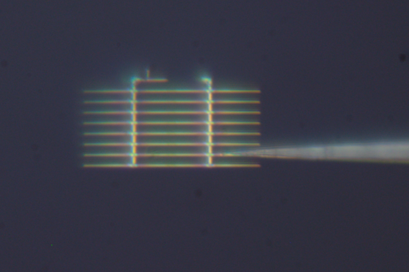 Microscope photograph of a device that could jumpstart work toward the
quantum internet. The horizontal lines are diamond waveguides, each about 1,000 times
smaller than a human hair.Credit: Atatüre Laboratory, University of Cambridge
Microscope photograph of a device that could jumpstart work toward the
quantum internet. The horizontal lines are diamond waveguides, each about 1,000 times
smaller than a human hair.Credit: Atatüre Laboratory, University of Cambridge In research that could jumpstart work toward the quantum internet, researchers at MIT and the University of Cambridge have built and tested an exquisitely small device that could allow the quick, efficient flow of quantum information over large distances.
Key to the device is a “microchiplet” made of diamond in which some of the diamond’s carbon atoms are replaced with atoms of tin. The team’s experiments indicate that the device, consisting of waveguides for the light to carry the quantum information, solves a paradox that has stymied the arrival of large, scalable quantum networks.
Quantum information in the form of quantum bits, or qubits, is easily disrupted by environmental noise, like magnetic fields, that destroys the information. So on one hand, it’s desirable to have qubits that don’t interact strongly with the environment. On the other hand, however, those qubits need to strongly interact with the light, or photons, key to carrying the information over distances.
The MIT and Cambridge researchers allow both by co-integrating two different kinds of qubits that work in tandem to save and transmit information. Further, the team reports high efficiencies in the transfer of that information.
“This is a critical step as it demonstrates the feasibility of integrating electronic and nuclear qubits in a microchiplet. This integration addresses the need to preserve quantum information over long distances while maintaining strong interaction with photons. This was possible through the combination of the strengths of the University of Cambridge and MIT teams,” says Dirk Englund, an associate professor in MIT’s Department of Electrical Engineering and Computer Science (EECS) and leader of the MIT team. Englund is also affiliated with MIT’s Materials Research Laboratory.
Says Professor Mete Atatüre, leader of the Cambridge team: “The results are an outcome of a strong collaborative effort between the two research teams over the years. It is great to see the combination of theoretical prediction, device fabrication, and the implementation of novel quantum optical controls all in one work.”
The work was reported in Nature Photonics. Coauthors from MIT are Kevin C. Chen, MIT PhD; Isaac B. Harris, an EECS graduate student; and Matthew E. Trusheim, a postdoctoral research scientist. Coauthors from Cambridge are Ryan A. Parker, Jesús Arjona Martínez, Alexander M. Stramma, Cathryn P. Michaels, Martin Hayhurst Appel, Carola M. Purser, and William G. Roth. Parker and Martínez are co-first authors of the paper.
Working at the Quantum Scale
A computer bit can be thought of as anything with two different physical states, such as “on” and “off,” to represent zero and one. In the strange ultra-small world of quantum mechanics, a qubit “has the extra property that instead of being in just one of these two states, it can be in a superposition of the two states. So it can be in both of those states at the same time,” says Martínez. Multiple qubits that are entangled, or correlated with each other, can share much more information than the bits associated with conventional computing. Hence the potential power of quantum computers.
There are many kinds of qubits, but two common types are based on spin, or the rotation of an electron or a nucleus (left to right, or right to left). The new device involves both electronic and nuclear qubits.
A spinning electron, or electronic qubit, is very good at interacting with the environment, while the spinning nucleus of an atom, or nuclear qubit, is not. “We’ve combined a qubit that is well known for interacting easily with light with a qubit that is well known for being very isolated, and thus preserving information for a long time. By combining these two, we think we can get the best of both worlds,” says Martínez.
How does it work? “The electron [electronic qubit] whizzing along in the diamond can get stuck at the tin defect,” says Harris. And this electronic qubit can then transfer its information to the spinning tin nucleus, the nuclear qubit.
“The analogy I like to use is the solar system,” Harris continues. “You have the Sun in the middle, that’s the tin nucleus, and then you have the Earth going around it, and that’s the electron. We can choose to store the information in the direction of the Earth’s rotation, that’s our electronic qubit. Or we can store the information in the direction of the Sun, which rotates around its own axis. That’s the nuclear qubit.”
In general, then, light carries information through an optical fiber to the new device, which includes a stack of several tiny diamond waveguides that are each about 1,000 time smaller than a human hair. Several devices, then, could act as the nodes that control the flow of information in the quantum internet.
The work described in Nature Photonics involves experiments with one device. “Eventually, however, there could be hundreds or thousands of these on a microchip,” Martínez says. In a paper that appeared in Nature, MIT researchers, including several of the current authors, describe their vision for the architecture that will enable the large-scale integration of the devices.
Some Personal Highlights
What was the best part of working on this project? Harris notes that his theoretical work had predicted a strong interaction between the tin nucleus and the incoming electronic qubit. “It was ten times larger than we expected it to be, so I thought the calculation was probably wrong. Then the Cambridge team came along and measured it, and it was neat to see that the prediction was confirmed by the experiment.”
Agrees Martínez, “the theory plus the experiments finally convinced us that [these interactions] were really happening.”
This work was funded by the European Research Council, the Winton Programme, the Engineering and Physical Sciences Research Council, the General Sir John Monash Foundation, the MITRE Quantum Moonshot Program, and the Army Research Laboratory.
Media Inquiries
Journalists seeking information about EECS, or interviews with EECS faculty members, should email eecs-communications@mit.edu.
Please note: The EECS Communications Office only handles media inquiries related to MIT’s Department of Electrical Engineering & Computer Science. Please visit other school, department, laboratory, or center websites to locate their dedicated media-relations teams.