Pushing the limits of electronic circuits
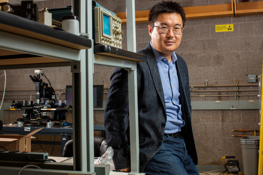
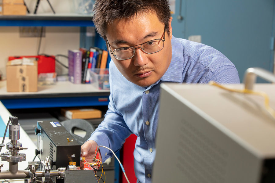
 Ruonan Han, associate professor in the Department of Electrical Engineering and Computer Science, seeks to push the limits of electronic devices so they can operate efficiently at terahertz frequencies.
Photo credits: M. Scott Brauer
 Ruonan Han’s research is driving up the speeds of microelectronic circuits to enable new applications in communications, sensing, and security.
Han, an associate professor who recently earned tenured in MIT’s Department of Electrical Engineering and Computer Science, focuses on producing semiconductors that operate efficiently at very high frequencies in an effort to bridge what is known as the “terahertz gap.”
The terahertz region of the electromagnetic spectrum, which lies between microwaves and infrared light, has largely eluded researchers because conventional electronic devices are too slow to manipulate terahertz waves.
“Traditionally, terahertz has been unexplored territory for researchers simply because, frequency-wise, it is too high for the electronics people and too low for the photonics people,” he says. “We have a lot of limitations in the materials and speeds of devices that can reach those frequencies, but once you get there, a lot of amazing things happen.”
For instance, terahertz frequency waves can move through solid surfaces and generate very precise, high-resolution images of what is inside, Han says.
Radio frequency (RF) waves can travel through surfaces, too — that’s the reason your Wi-Fi router can be in a different room than your computer. But terahertz waves are much smaller than radio waves, so the devices that transmit and receive them can be smaller, too.
Han’s team, along with his collaborator Anantha Chandrakasan, dean of the School of Engineering and the Vannevar Bush Professor of Electrical Engineering and Computer Science, recently demonstrated a terahertz frequency identification (TFID) tag that was barely 1 square millimeter in size.
“It doesn’t need to have any external antennas, so it is essentially just a piece of silicon that is super-cheap, super-small, and can still deliver the functions that a normal RFID tag can do. Because it is so small, you could now tag pretty much any product you want and track logistics information such as the history of manufacturing, etc. We couldn’t do this before, but now it becomes a possibility,” he says.
Tuning in
A simple radio inspired Han to pursue engineering.
As a child in Inner Mongolia, a province that stretches along China’s northern border, he pored over books filled with circuit schematics and do-it-yourself tips for making printed circuit boards. The primary school student then taught himself to build a radio.
“I couldn’t invest a lot into those electronic components or spend too much time tinkering with them, but that was where the seed was planted,” he says. “I didn’t know all the details of how it worked, but when I turned it on and saw all the components working together it was really amazing.”
Han studied microelectronics at Fudan University in Shanghai, focusing on semiconductor physics, circuit design, and microfabrication.
Rapid advances from Silicon Valley tech companies inspired Han to enroll in a U.S. graduate school. While earning his master’s degree at the University of Florida, he worked in the lab of Kenneth O, a pioneer of the terahertz integrated circuits that now drive Han’s research.
“Back then, terahertz was considered to be ‘too high’ for silicon chips, so a lot of people thought it was a crazy idea. But not me. I felt really fortunate to be able to work with him,” Han says.
He continued this research as a PhD student at Cornell University, where he honed innovative techniques to supercharge the power that silicon chips can generate in the terahertz domain.
“With my Cornell advisor, Ehsan Afshari, we experimented with different types of silicon chips and innovated many mathematics and physics ‘hacks’ to make them run at very high frequencies,” he says.
As the chips became smaller and faster, Han pushed them to their limits.
Making terahertz accessible
Han brought that innovative spirit to MIT when he joined the EECS faculty as an assistant professor in 2014. He was still pushing the performance limits of silicon chips, now with an eye on practical applications.
“Our goal is not only to work on the electronics, but to explore the applications that these electronics can enable, and demonstrate the feasibility of those applications. One especially important aspect of my research is that we don’t just want to deal with the terahertz spectrum, we want to make it accessible. We don’t want this to just happen inside labs, but to be used by everybody. So, you need to have very low-cost, very reliable components to be able to deliver those kinds of capabilities,” he says.
Han is studying the use of the terahertz band for rapid, high-volume data transfer that could push wireless devices beyond 5G. The terahertz band could be useful for wired communications, too. Han recently demonstrated the use of ultrathin cables to transmit data between two points at a speed of 100 gigabits per second.
Terahertz waves also have unique properties beyond their applications in communications devices. The waves cause different molecules to rotate at unique speeds, so researchers can use terahertz devices to reveal the composition of a substance.
“We can actually make low-cost silicon chips that can ‘smell’ a gas. We’ve created a spectrometer that can simultaneously identify a large range of gas molecules with very low false alarms and high sensitivity. This is something that the other spectrum is not good at,” he says.
Han’s team drew on this work to invent a molecular clock that turns the molecular rotation rate into a highly stable electrical timing signal for navigation, communication, and sensing systems. Although it functions much like an atomic clock, this silicon chip has a simpler structure and greatly reduced cost and size.
Operating in largely unexplored areas makes this work especially challenging, Han says. Despite decades of advances, semiconductor electronics still aren’t fast enough, so Han and his students must constantly innovate to reach the level of efficiency required for terahertz devices.
The work also requires an interdisciplinary mindset. Collaborating with colleagues in other domains, such as chemistry and physics, enables Han to explore how the technology can lead to useful new applications.

Han is glad he’s at MIT, where the students aren’t afraid to take on seemingly intractable problems and he can collaborate with colleagues who are doing incredible research in their domains.
“Every day we are facing new problems and thinking about ideas that other people, even people who work in this field, may consider super-crazy. And this field is in its infancy right now. There are a lot of new emerging materials and components, and new needs and potential applications keep popping up. This is just the beginning. There are going to be very big opportunities lying ahead of us,” he says.
Media Inquiries
Journalists seeking information about EECS, or interviews with EECS faculty members, should email eecs-communications@mit.edu.
Please note: The EECS Communications Office only handles media inquiries related to MIT’s Department of Electrical Engineering & Computer Science. Please visit other school, department, laboratory, or center websites to locate their dedicated media-relations teams.