
Nano flashlight could allow future cell phones to detect viruses, more

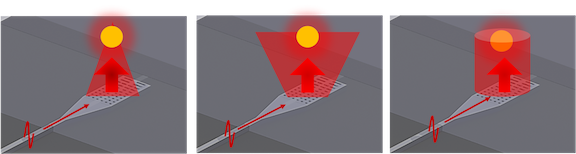
Schematic of three different nano flashlights for the generation of, left to right, focused, wide-spanning, and collimated beams. Each could have different applications. Schematic courtesy Robin Singh.
In work that could turn cell phones into sensors capable of detecting viruses and other minuscule objects, MIT researchers have built a powerful nanoscale flashlight on a chip. Their approach could also be used to create a variety of other nano flashlights with different beam characteristics for different applications. Think of a wide spotlight versus a beam of light focused on a single point.
Scientists have long used light to identify a material by observing how that light interacts with the material. They do so by essentially shining a beam of light on the material, then analyzing that light after it passes through the material. Because all materials interact with light differently, an analysis of the light that passes through the material provides a kind of “fingerprint” for that material. Imagine doing this for several colors, i.e. several wavelengths of light, and capturing the interaction of light with the material for each color. That would lead to a fingerprint that is even more detailed.
Most instruments for doing this, known as spectrometers, are relatively large. Making them much smaller would have a number of advantages. For example, they could be portable and have additional applications (imagine a futuristic cell phone loaded with a self-contained sensor for a specific gas). However, while researchers have made great strides towards miniaturizing the sensor for detecting and analyzing the light that has passed through a given material, a miniaturized and appropriately shaped light beam—or flashlight—remains a challenge. Today that light beam is most often provided by macroscale equipment like a laser system that is not built into the chip itself as the sensors are.
Enter the MIT work. In two recent papers in Nature Scientific Reports, the team describes not only their approach for designing on-chip flashlights with a variety of beam characteristics, they also report building and successfully testing a prototype. Importantly, they created the device using existing fabrication technologies familiar to the microelectronics industry, so they are confident that the approach could be deployable at a mass scale with the lower cost that implies.
Complete Sensor
Overall, this could enable industry to create a complete sensor on a chip with both light source and detector. As a result, the work represents a significant advance in the use of silicon photonics for the manipulation of light waves on microchips for sensor applications.
“This work is significant, and represents a new paradigm of photonic device design, enabling enhancements in the manipulation of optical beams,” says Dawn Tan, an associate professor at the Singapore University of Technology and Design who was not involved in the research.
“Silicon photonics has so much potential to improve and miniaturize the existing bench-scale biosensing schemes. We just need smarter design strategies to tap its full potential. This work shows one such approach,” says Robin Singh, lead author of both papers. Singh received the MS (2018) and PhD (2020) from MIT, both in mechanical engineering.
The senior coauthors on the first paper are Anuradha Murthy Agarwal, a principal research scientist in MIT’s Materials Research Laboratory, and Brian W. Anthony, a principal research scientist in MIT’s Department of Mechanical Engineering. Singh’s coauthors on the second paper are Agarwal; Anthony; Yuqi Nie, now at Princeton University; and Mingye Gao, a graduate student in MIT’s Department of Electrical Engineering and Computer Science.
How They Did It
Singh and colleagues created their overall design using multiple computer modeling tools. These included conventional approaches based on the physics involved in the propagation and manipulation of light, and more cutting-edge machine-learning techniques in which the computer is taught to predict potential solutions using huge amounts of data. “If we show the computer many examples of nano flashlights, it can learn how to make better flashlights,” says Anthony. Ultimately, “we can then tell the computer the pattern of light that we want, and it will tell us what the design of the flashlight needs to be.”
All of these modeling tools have advantages and disadvantages; together they resulted in a final, optimal design that can be adapted to create flashlights with different kinds of light beams.
The researchers went on to use that design to create a specific flashlight with a collimated beam, or one in which the rays of light are perfectly parallel to each other. Collimated beams are key to some types of sensors. The overall flashlight that the researchers made involved some 500 rectangular nanoscale structures of different dimensions that the team’s modelling predicted would enable a collimated beam. Nanostructures of different dimensions would lead to different kinds of beams that in turn are key to other applications.
Singh describes the excitement he felt upon creating that first flashlight. “It was great to see through a microscope what I had designed on a computer. Then we tested it, and it worked!” The tiny flashlight with a collimated beam worked. Not only that, it provided a beam that was five times more powerful than is possible with conventional structures. That’s partly because “being able to control the light better means that less is scattered and lost,” says Agarwal.
This research was supported in part by the MIT Skoltech Initiative.
As a Principal Research Scientist in the Microphotonics Center and the Initiative for Knowledge and Innovation in Manufacturing (IKIM), Agarwal acknowledges her colleagues for providing the fertile intellectual environment for this work.
Additional MIT facilities and departments that made this work possible are the Department of Materials Science and Engineering, the Materials Research Laboratory, the Institute for Medical Engineering & Science, and MIT.nano.
Media Inquiries
Journalists seeking information about EECS, or interviews with EECS faculty members, should email eecs-communications@mit.edu.
Please note: The EECS Communications Office only handles media inquiries related to MIT’s Department of Electrical Engineering & Computer Science. Please visit other school, department, laboratory, or center websites to locate their dedicated media-relations teams.